| Australian National Fabrication Facility | |
| Latest News |
September 2011
A tremendous amount of research is being carried out in the field of nanowires and the excitement in this field is due to the unique properties of these nanowires. Nanowires have an extremely large surface area which leads to ultra high surface reaction efficiency. Changing the surface conditions by surface reactions with chemicals, gases and biological substances, including DNA/viruses, can lead to large changes in nanowire properties with ultra-sensitive sensors based on nanowires being reported.
Nanowire devices such as lasers, resonant tunnelling diodes, single electron transistors, photodetectors, and solar cells have also been demonstrated. Indeed, nanowires have a broad range of applications, which encompasses many science and engineering areas such as electronics, photonics, biological and medical technologies. The success of nanowires as building blocks for nano-devices relies not only on the synthesis of these materials but also the ability to fabricate them on the nano-scale into devices.
In this article, photoconductors based on Indium Phosphide (InP) nanowires were fabricated using various facilities of the ANFF ACT Node. The 50nm diameter InP nanowires were grown using the Au-catalysed technique by MOCVD with lengths varying from 4-15µm. After growth, the nanowires were removed from the substrate by sonication for 10 to 20 seconds in isopropanol. 200nm of SiOx was deposited on a Si substrate at 600°C by PECVD using the ACT Node's Oxford Instruments PlasmaLab 100 machine. Optical lithography was carried out to define regions of contact pads on the substrate. Ti/Au (5nm/200nm) was then deposited on the patterned substrate using the Temescal BJD-2000 Electron Beam Evaporator followed by acetone lift-off process.
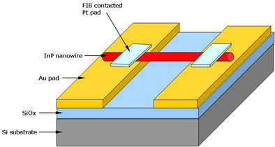
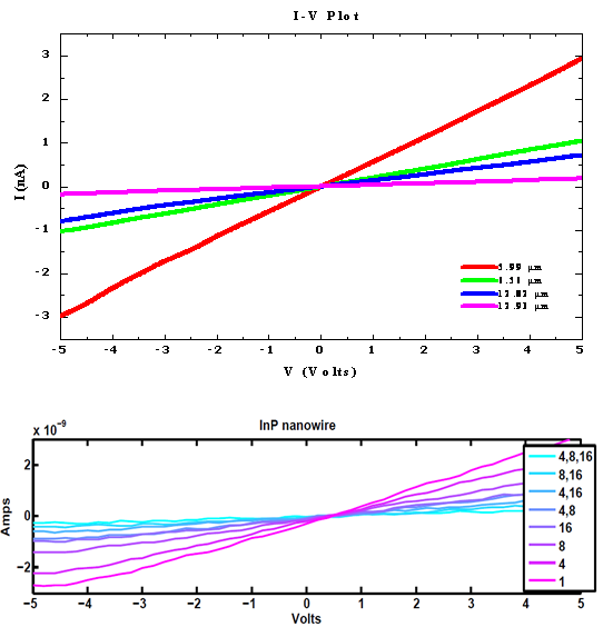
The isopropanol suspension containing the InP nanowires was then applied on the patterned wafer. Many nanowires were found dispersed on the patterned substrate upon evaporation of the isopropanol solution. By choosing nanowires that lie across two Au contact pads, further contacts were made using the FEI Helios 600 NanoLab Focused Ion Beam system. Gallium ion-induced Pt deposition was used to bond the nanowires onto the Au pads. A schematic of the device structure is shown in Figure 1, whilst Figure 2 shows the SEM image of a typical nanowire device. Electrical measurements show a linear current-voltage relationship, indicating the formation of Ohmic contacts (see Figure 3a) for all lengths of nanowires studied here. The results of optical excitation using a 522nm laser are shown in Figure 3b.
 |
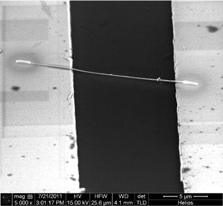 |
Figure 1: Schematic of InP nanowire (red bar) contacted by FIB Pt |
Figure 2: Field Emission Scanning Electron Microscopy (FE-SEM) |
 |
|
| Figure 3a (top): Current-voltage characteristics of FIB Pt contacted InP nanowires having different lengths. Fig 3b (above) shows current-voltage relationship with different laser powers, 1 being the maximum laser power (measured as 717μJcm-2) and (4,8,16) the minimum laser power. 4,8,16 denote for neutral density filters. | |
By increasing the intensity of the excitation beam, an increase in the photocurrent is observed, while still preserving the Ohmic contacts. The successful demonstration of these devices shows that the fabrication techniques used are feasible and reliable. It also allows us to venture into more exciting structures such as axial and radial (core-shell) heterostructures.
However, it is worth noting ion beam deposition conditions such as deposition time, dimensions and current must be carefully optimised to avoid/minimise gallium ion generated artefacts such as Pt spill over, sputtering around the contact areas, device short circuiting from Pt spreading and ion beam induced damage. More systematic experiments and analysis need to be carried out to investigate the relationship between the NW structural properties (length, diameter, crystallography, etc) and the electrical properties of the NWs.
Story courtesy of Prakash Prasai, PhD student in the Department of Electronic Materials Engineering, Research School of Physics & Engineering, The Australian National University.
|
|
|
Page last updated:
6 November, 2014
|
||