| Australian National Fabrication Facility | |
| Latest News |
September 2012
Researchers at the Department of Electronic Materials Engineering (EME) at ANU have been working on III-V semi-conductor nanowires that offer the possibility of achieving even higher density integration of optoelectronic devices (such as LEDs, lasers and photo-detectors) than current planar devices via the use of their inherent 3-dimesional type architecture.
High quantum efficiency (QE) in semi-conductors is essential for making efficient optoelectronic devices (QE is defined as the ratio of the radiative recombination rate and total recombination rate (both radiative and non-radiative)). A large surface area to volume ratio results in very poor quantum efficiencies in the nanowires due to non-radiative surface recombination, despite very good material quality. High quantum efficiencies in nanowires can be achieved by either reducing the non-radiative rate or by increasing the radiative rate. The non-radiative recombination rate can be reduced by quenching the surface states through surface passivation and this approach is actively being pursued for nanowire optoelectronic devices. The EME researchers approach for making opto-electronic device quality nanowires is to increase radiative recombination rate by coupling the nanowires to plasmonic structures.
 |
 |
 |
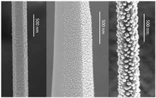
| Figure 1: Different configurations for integrating nanowires with plasmonic structures. Left: Continuous film of Ag deposited on a nanowire surface using thermal evaporator; Centre: Ag nanoparticles deposited on selected facets of the nanowire using sputter deposition system without substrate rotation and Right: Ag nanoparticles deposited on all facets of a nanowire using sputter deposition system with substrate rotation. |
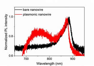
Figure 2: Plasmonic nanowires show distinctly different optoelectronic characteristics, where enhanced light efficiency due to coupling of the nanoparticles to the nanowire shell is observed. |
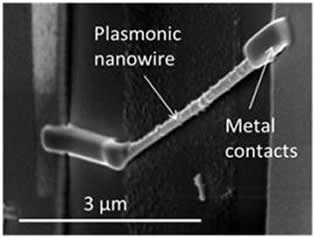
Figure 3: Plasmonic nanowires contacted using Pt electrodes deposited by FIB for electrical measurements. |
Dr Sudha Mokkapati and her colleagues have been successful in integrating plasmonic structures with nanowires. Figure 1 shows three different configurations of coupled nanowire-plasmonic structures created from the deposition of silver (Ag) using the E-Beam Evaporator and Sputter Deposition System at the ANFF ACT Node facility. Depending on the deposition conditions, a conformal layer of nano-particles can be deposited on the nano-wires. Such structures support surface plasmon polaritons (SPPs) at the nanowire-metal interface. The discrete metal nano-particles support localised surface plasmons (LSPs) and the plasmon modes can increase the radiative recombination rate in the semi-conductor by concentrating electro-magnetic fields in the nanowire. This is analogous to the Purcell effect observed in dielectric resonant cavities. Nanowires coupled to plasmonic structures emit light much more efficiently compared to bare nanowires - Figure 2 shows light emission from GaAs core-AlGaAs shell nanowires. Bare nanowires show a single peak at 870nm from the GaAs core, however there is no emission from the AlGaAs shell in bare nanowires due to very low quantum efficiency of the shell. In nano-wires coupled to plasmonic structures the emission from AlGaAs shell is clearly seen at 730nm due to enhanced quantum efficiency. Devices have now been successfully fabricated from nanowires coupled to plasmonic structures by electrically contacting the nano-wires through platinum (Pt) deposited using the FIB system at ANFF-ACT, as shown in Figure 3.
These devices are currently being characterised and are expected to show superior performance compared to devices fabricated from bare nanowires.
|
|
|
Page last updated:
6 November, 2014
|
||