| Australian National Fabrication Facility | |
| Latest News |
March 2013
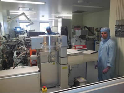 |
Sentech SI 500D Inductively Coupled Plasma Enhanced Chemical Vapour Deposition (ICPECVD) tool in full swing at the ANFF-WA fabrication facility. The tool is operated by postgraduate student Rohit Sharda. |
With the aid of the Educational Investment Fund (EIF), ANFF-Qld acquired a state-of-the-art thin film deposition tool. A Sentech SI 500D Inductively Coupled Plasma Enhanced Chemical Vapour Deposition (ICPECVD) system was supplied from Germany by SENTECH Instruments GmbH and represents the leading edge for plasma deposition. The tool features exceptional plasma properties such as high density and low ion energy. A uniquely designed Planar Triple Spiral Antenna (PTSA) ICP plasma source allows efficient power coupling leading to low stress film growth with no damage of substrate, very low interface state density down to deposition temperatures of less than 100°C allowing for outstanding properties of the deposited films. The substrate electrode with dynamic temperature control, in combination with He backside cooling and substrate backside temperature sensing, provides excellent stable process conditions over a wide temperature range from room temperature up to +300°C.
However installation turned out to be not possible at ANFF-Qld and, in a ANFF inter-node collaborative effort, the capability was transferred, installed and commissioned at ANFF-WA within the Western Australian Centre for Semiconductor Optoelectronics and Microsystems (WACSOM).
The SI 500D plasma enhanced deposition tool is configured to deposit SiO2, SiNx, SiOyNx and α-Si films in a temperature range from room temperature up to 300°C. The SI 500D is especially suited for the deposition of high efficient protection barriers on organic materials at low temperatures and damage free deposition of passivating films at well-defined temperatures. A large variety of substrates from wafers up to 8" (200mm) diameter to parts loaded on carriers can be processed. The single wafer vacuum loadlock guarantees stable process conditions and allows for easy switching between processes.
Story by Mariusz Martynuik, ANFF WA Node Manager.
|
|
|
Page last updated:
6 November, 2014
|
||