

Published in the ANFF ACT & WA Node Newsletter
Issue 47 - March 2021
Micromachining Porous Silicon: A Treasure Made of Air
Recent years have seen an increasing need for thermal imaging (night vision) cameras, which can enhance safety and emergency services, by detecting the thermal radiation (i.e. long wavelength infrared, LWIR: 8-12 µm) of targets. To date, high-performance thermal imaging cameras are typically bulky and expensive. Compared to other kinds of approaches, micromachined tuneable Fabry-Pérot filters offer miniaturisation and high optical throughput. Fabry-Pérot filter consists of two flat, reflective mirrors spaced a well-defined distance apart, where this space defines the resonant cavity oscillation wavelength. Mirrors formed using multiple layers of alternating refractive index are preferred in order to achieve high reflectivity. However, finding compatible materials from which to construct these mirrors can be very challenging, particularly for filters operating in the LWIR range, due to the limited materials having low-absorption in this range. Ideally, using a single material to build LWIR filters would eliminate the incompatibility issue and potentially lower costs, but a single material compromises the ability to achieve layers with a high index contrast, required for high reflectivity. Alternatively, engineering the refractive index of a single material could provide a powerful method to enhance optical design in the LWIR range.
A porous silicon team, led by Professor Adrian Keating and Professor Gia Parish at the University of Western Australia, has been investigating micromachining porous silicon (PS) for a range of sensors applications. PS is a unique material that exhibits a range of interesting properties, offering much potential in constructing the next generation of micromachined LWIR filters. One property is the ability to form thick PS layers with alternating refractive indices by modulating the porosity during the anodisation process. Another property is the ability to release the mirrors using an electrochemical etching step, allowing suspended filters with an air gap to be formed. This single material system provides a pathway to produce suspended mirrors having high reflectivity and low optical loss, and being relatively mechanically rigid. Importantly, being an all-silicon material system, PS is compatible with conventional semiconductor technologies and fabrication techniques, leading to mass-production capabilities.
Nonetheless, while formation of multilayer PS can be achieved by a simple anodisation process, surface-micromachining PS (the technology of making structures out of thin films extending above a substrate) has not been simple. The porous nature has caused challenges throughout every step of the micromachining process, as well as in characterisation of the final device. Below are three examples demonstrating the challenges in fabricating and characterising micromachined PS, and how these challenges were resolved by the work of Yaman Afandi, a PhD student in the porous silicon team. Details of the developed process to micromachine PS and the characterisation of the final device will be published in the near future.
Air Cavity Formation
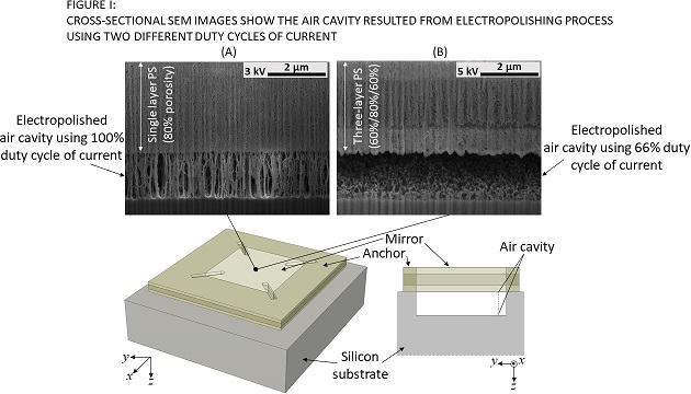
In the LWIR, formation of an air cavity between the top mirror PS and the silicon substrate requires a height of nominally 5 µm. Electropolishing is a very common process to detach PS thin films from the silicon substrate, a process based on applying high current density and using a low concentration of hydrofluoric acid in the anodisation electrolyte. For the developed micromachining process, distilled water was used to dilute hydrofluoric acid (instead of ethanol, which enhances the diffusivity of hydrofluoric into the underlying pores), resulting in partial electropolishing successful, as shown in Figure 1A. To address this issue, pulsing the electropolishing current was utilised to provide sufficient time for the hydrofluoric concentration to be restored at the PS/silicon interface. Using a 66% duty cycle for current during electropolishing allowed successful air cavity formation, as shown in Figure 1B, with a yield of 4%. Lowering the duty cycle to 50% resulted in a high yield of 50%.
Cross-sectional images
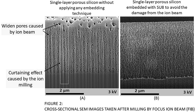
Characterising films with porosities approaching 80% was extremely challenging due to its low Young’s Modulus of around 1GPa. To obtain high resolution cross-sectional images, the typical method to cleave PS samples was not preferable, as it results in fractures and makes interpreting the porosity inaccurate. A focussed ion beam (FIB) was used to slice through the PS films. However, there are two major challenges related to the FIB procedure for PS: a curtaining effect (vertical striations) and degradation of the top surface quality. As a result, the SEM image shown in Figure 2A incorrectly represents the morphology of the material – no columnar structure is actually present in these films. To resolve these issues, the pores were filled with epoxy (SU8) to provide protection during exposure to the ion beam. After immersing PS in SU8, the sample was cycled under vacuum a few times to ensure complete pore filling and then the sample was baked at very high temperature to harden the SU8. As a result, clear images of the pores throughout the film were obtained, as shown in Figure 2B.
Stress measurement
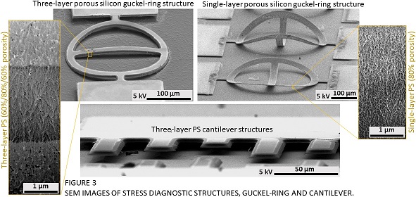
Measuring the mechanical properties of the final device is important to determine the flatness and to assess the performance of the device. Guckel-rings and cantilevers are typically used as diagnostic micromachined structures to determine film stress, evaluated by measuring the deflection of the structures. Although those structures where successfully formed in single-layer and 3-layer PS films (notice that the complete suspended structures were made of pores), as shown in Figure 3, evaluating the stress could not be measured as the surface profile could not able to be obtained using a standard optical profilometer. It is known that optical profilometers measure fringes, working well on highly reflective surfaces and/or thick, low-loss films. However the low reflectivity and transparency of our PS films, suspended in air resulted in significant interference fringes, making accurate determination of the film deflection impossible. To resolve this issue, the residual stress was measured by obtaining the resonance frequency using an optical laser Doppler vibrometer to extract the stress and Young’s modulus in PS cantilevers. The resonance measurements showed that 3-layer PS structures exhibited an extremely low tensile stress of 0.1 MPa with effective Young’s modulus of 3.32 GPa. This impressive result indicates that the overall strain of micromachined PS was lower than reported values of amorphous silicon and polysilicon thin films, which are widely used in micro-electro-mechanical systems (MEMS) due to their favourable mechanical properties.
In conclusion, several challenges were addressed to develop a successful process to micromachine PS Fabry-Pérot filters, operating in the long wavelength infrared range, along with characterisation of the final device. This work provides methods to fabricate potentially tuneable, optically flat micromachined multilayer structures for LWIR applications, using a low-cost single base material (silicon). Furthermore, the findings are a good starting point for the future development of miniature, multispectral thermal imaging systems incorporating a large-area MEMS-based filters.
Article written by, Yaman Afandi, UWA