
ANFF ACT Tools and Capabilities
| Nano-Patterning | Chemical Vapour Deposition |
|---|---|
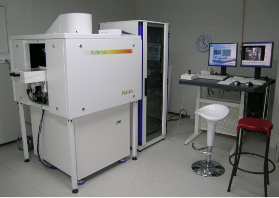
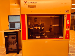
Electron Beam Lithography (EBL-Elionix) Electron Beam Lithography (EBL-Raith) Maskless Aligner (MLA150) (MLA150) Nano-imprint Lithography (EVG620 NIL) Hot-Embossing (EVG520HE) |
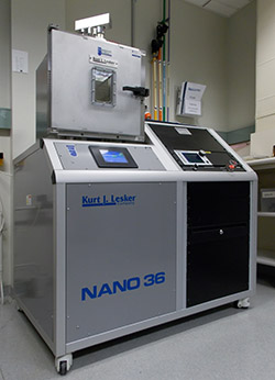
Metal Organic Chemical Vapour Deposition (MOCVD GaAs) Metal Organic Chemical Vapour Deposition (MOCVD GaN) Metal Organic Chemical Vapour Deposition (MOCVD) Plasma Enhanced Chemical Vapour Deposition (PECVD) Plasma - Atomic Layer Deposition (P-ALD) |
| Metrology and Characterization | Physical (Vapour) Deposition |
|---|---|
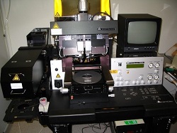
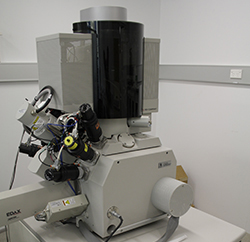
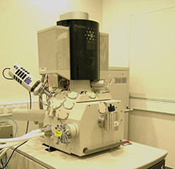
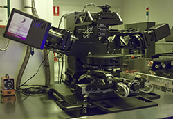
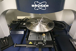
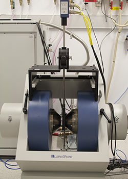
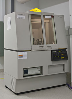
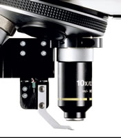
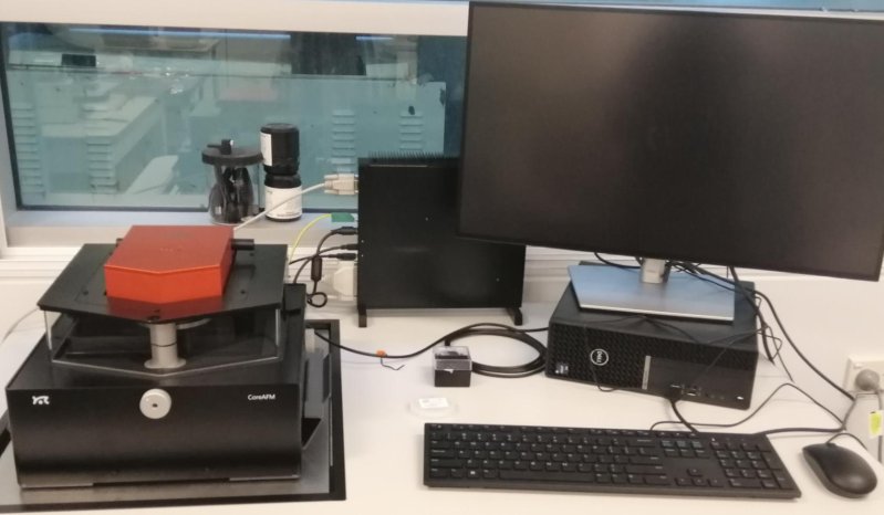
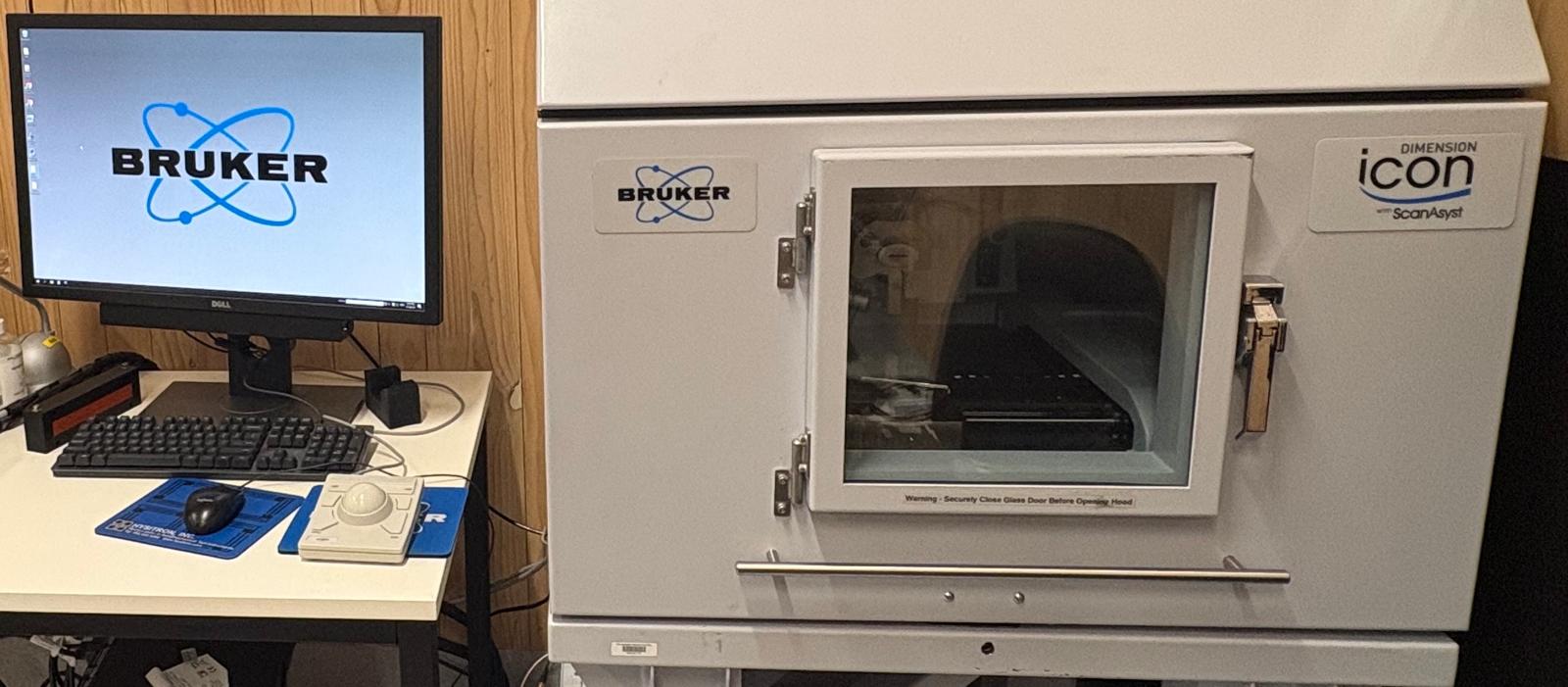
Focused Ion Beam (FIB) Scanning Electron Microscope (SEM-CL) X-ray Diffractometer (XRD) Scanning Near-Field Optical Microscope WiTec Atomic Force Microscope - NanoSurf (AFM-N) Atomic Force Microscope - Bruker (AFM-B) |
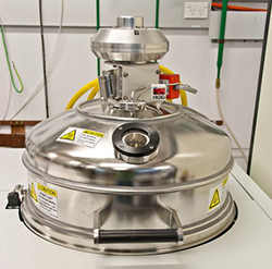
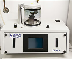
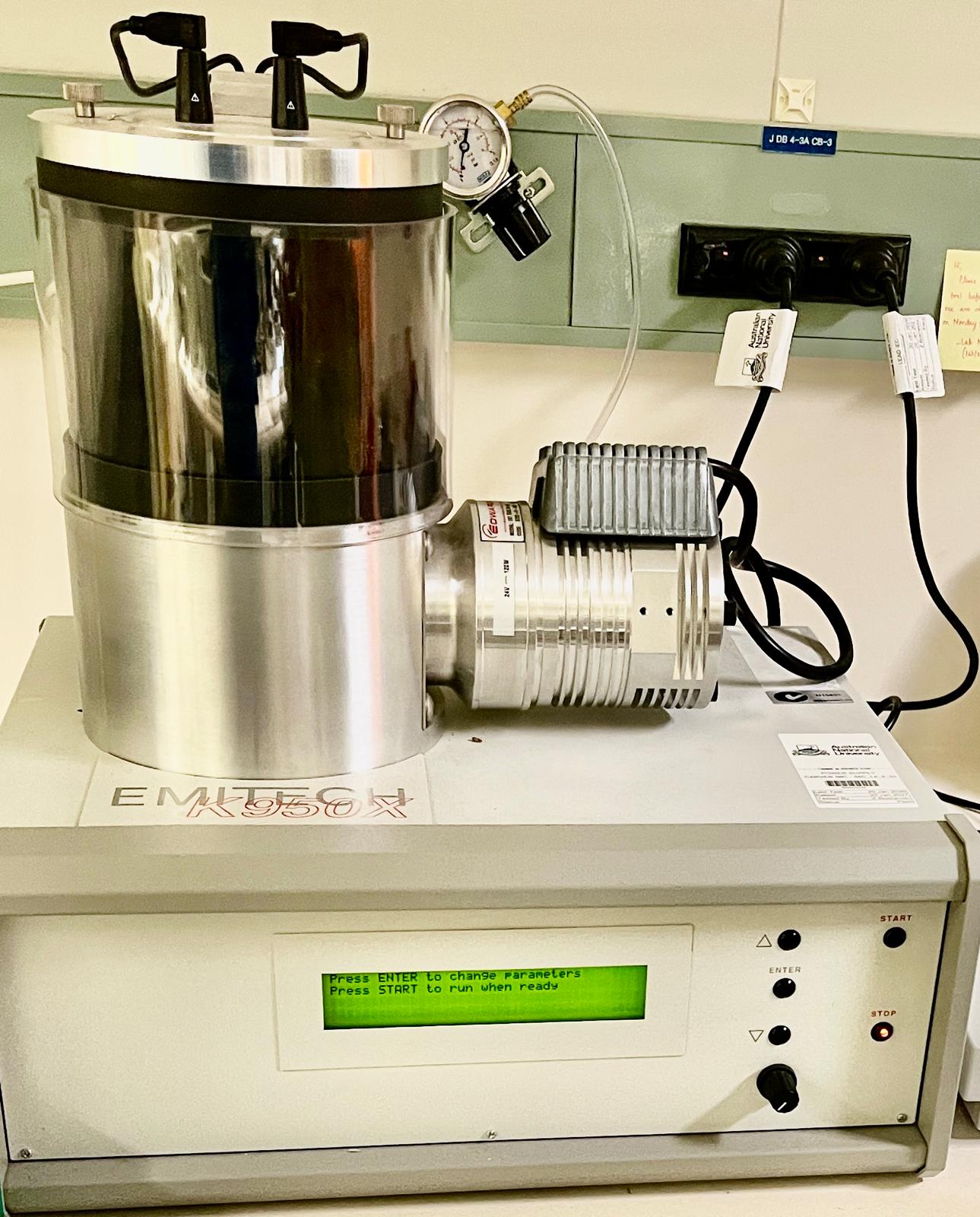
Electron Beam Evaporator (EB-Evap) Thermal Evaporator (TE) Desktop Sputter Coater - Au, Pd Parylene Coating (P6) |
| Modification and Packaging | Dry Etching |
|---|---|
|
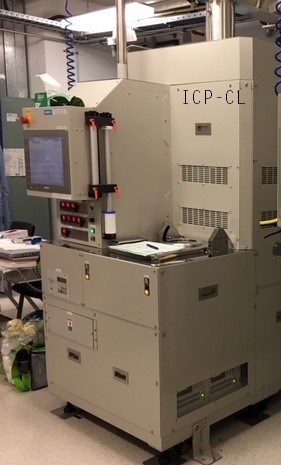
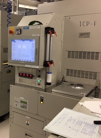
Inductively Coupled Plasma Etching (ICP-CL) Inductively Coupled Plasma Etching (ICP-F) Barrel Etcher/Plasma Asher |
| Implanter (AFAiiR) |
|---|
|
High Energy Low Engery Rutherford Back Scattering |
.jpg)

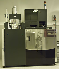


| Implanter (AFAiiR) | |
|---|---|
Ion Implanters - High Energy, Low Energy and RBSFor full details on the Ion Implanters please have a look at the Australian Facility for Advanced Ion Implanter Research website here The High Energy Implanter features a 1.7MV tandem accelerator incorporating a 100kV injector with a SNICS II negative ion sputter source. Used for implanting ions in the energy range 15-100keV (using the injector only) and 200keV to several MeV (depending on selected ion charge state). Most ions are available but implant fluences may be limited in some cases. Typical samples sizes are a few cm square but wafers up to 100mm diameter can be accommodated (150mm wafer chamber currently under construction). Smaller samples can be heated to 700°K or cooled to 77°K during implantation. The Low Energy Implanter features a 175kV accelerator with a SNICS II negative ion sputter source. Used for ion-implanting materials with energetic ions in the energy range 10keV to 175keV. Typical samples sizes are a few cm square but wafers up to 100mm diameter can be accommodated. Many ions are available, including most standard dopants. Smaller samples can be heated to 700°K or cooled to 77°K during implantation. The Rutherford Backscattering Spectrometry (RBS) system features a 1.7MV tandem accelerator incorporating a 60kV injector with an Alphatross ion source. Used for ion-beam analysis of materials with energetic He+ and H+ beams (typically 1-3 MeV). Standard techniques include Rutherford backscattering and channelling analysis (RBS-C) and elastic recoil detection (ERD) for hydrogen profiling. Particle-induce x-ray analysis (PIXE) is currently under development. Typical sample sizes range from 5mm square to several centimetres square. |
Low Energy Implanter
High Energy Implanter
Ion Beam Analysis (RBS, ERDA, PISIE) |


For a full, searchable listing of Australia-wide ANFF capabilities and equipment, visit the ANFF HQ web page.